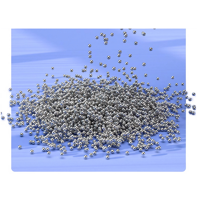
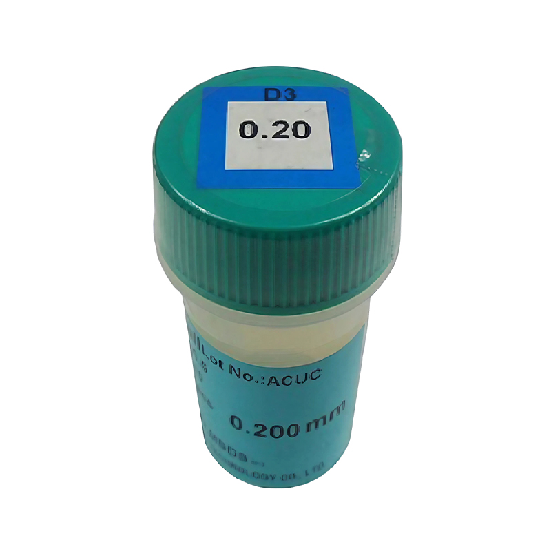
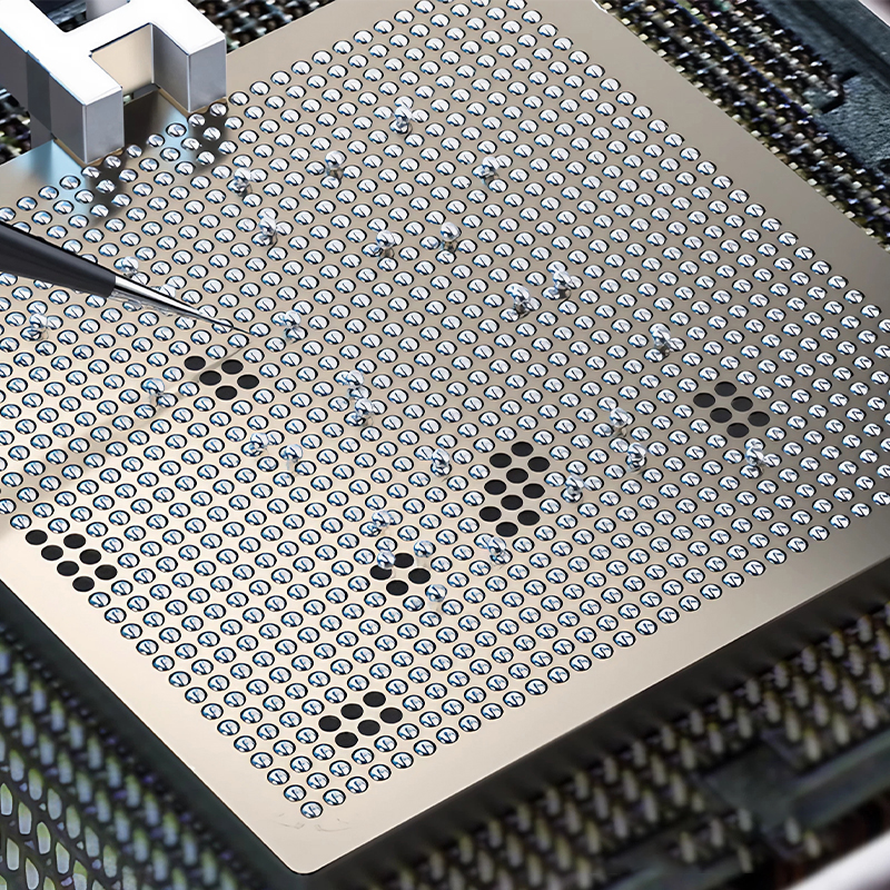
In smartphones, high-performance computing chips, communication base stations, and even aerospace electronic systems, the integration density of integrated circuits is increasing at an astonishing rate.
Within smartphone chip packages, on high-performance server motherboards, and between tiny solder joints in automotive electronic control units, a metal ball less than one millimeter in diameter silently undertakes the dual mission of electrical interconn
Without this exacting standard of sphericity, the reliability of advanced packaging would crumble, leaving the promise of next-generation electronics unfulfilled.
The relentless pursuit of miniaturization in the semiconductor industry has driven the development of ultra-high-density interconnects, where thousands of electrical connections are packed into microscopic areas. In this regime, the margin for error vanis
In the field of high-density electronic packaging, the solder ball, as a core interconnect component in advanced packaging forms such as BGA and CSP, directly determines the soldering quality and process yield.
In advanced electronic packaging technologies, especially in high-density interconnect structures such as ball grid arrays, chip-level packaging, and flip chips, the solder ball, as the core electrical and mechanical connection medium, directly determines